| CPC G06F 3/04184 (2019.05) [G02F 1/1345 (2013.01); G02F 1/13338 (2013.01); G06F 3/0412 (2013.01); G09G 3/2096 (2013.01); G09G 3/32 (2013.01); G09G 3/3677 (2013.01); H10K 50/844 (2023.02); H10K 50/865 (2023.02); H10K 59/40 (2023.02); G02F 1/133512 (2013.01); G09G 2300/0408 (2013.01); G09G 2300/0426 (2013.01); G09G 2310/0286 (2013.01)] | 18 Claims |

|
1. A display apparatus, comprising:
a timing controller, wherein the timing controller includes:
an integrated circuit chip configured to generate a reference clock signal, and to obtain at least one group of clock signals according to the reference clock signal, wherein each group of clock signals includes at least two clock signals, and a waveform of each clock signal is the same as a waveform of the reference clock signal, and active levels in different clock signals have a delay of a preset duration therebetween;
the reference clock signal includes a first clock sub-signal that lasts for a first duration and a second clock sub-signal that lasts for a second duration, a period of the first clock sub-signal is a first period, a period of the second clock sub-signal is a second period, the first clock sub-signal and the second clock sub-signal are adjacent, and a sum of the first period and the second period equals to a period of an image frame; and
at least one output interface group connected to the integrated circuit chip, wherein each output interface group includes at least two output interfaces, and each of the at least two output interfaces is configured to output one clock signal of a group of clock signals corresponding to the output interface group; and
a display panel including an array substrate, wherein the array substrate includes:
a first base substrate;
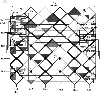
at least one clock signal line group provided on the first base substrate, wherein each clock signal line group includes at least two clock signal lines, and the at least two clock signal lines of the clock signal line group are connected to at least two output interfaces of one output interface group in one-to-one correspondence; and
a touch structure layer provided at a side of the at least one clock signal line group away form the first base substrate, wherein along a thickness direction of the first base substrate, an orthographic projection of the touch structure layer on the first base substrate overlaps with an orthographic projection of at least one clock signal line of the at least one clock signal line group on the first base substrate.
|