| CPC G02F 1/133531 (2021.01) [G02B 1/111 (2013.01); G02F 1/13439 (2013.01); G02F 1/133512 (2013.01)] | 15 Claims |
|
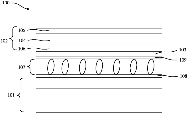
1. A display panel, comprising:
an array substrate,
an optical function layer located on the array substrate, wherein the optical function layer includes a second base substrate, a polarizing layer located on a side of the second base substrate away from the array substrate, and a second common electrode layer located on a side of the second base substrate close to the array substrate;
a liquid crystal layer located between the array substrate and the second common electrode layer;
a first alignment layer located on a side of the liquid crystal layer close to the array substrate;
a second alignment layer located on a side of the liquid crystal layer close to the second common electrode layer; and
an anti-reflection layer, wherein the anti-reflection layer and the first alignment layer are disposed within the same layer, or the anti-reflection layer is located between the first alignment layer and the array substrate,
wherein material of the anti-reflection layer includes a sulfur-containing material; and
wherein a refractive index of the anti-reflection layer is between refractive indexes of two film layers adjacent to the anti-reflection layer.
|