| CPC H10N 70/041 (2023.02) [H01L 21/67248 (2013.01); H01L 22/14 (2013.01); H10N 70/023 (2023.02); H10N 70/231 (2023.02); H10N 70/8828 (2023.02)] | 20 Claims |
|
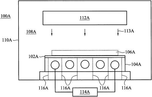
1. A method, comprising:
growing a phase change material on a platform configured for a semiconductor workpiece process;
setting the phase change material to an amorphous state;
performing the semiconductor workpiece process within a semiconductor processing chamber, wherein the semiconductor workpiece process comprises at least one of: rapid thermal processing (RTP), physical vapor deposition (PVD) or dynamic surface annealing (DSA); and
measuring a resistance across two points along the phase change material, wherein the resistance is measured across the two points while performing the semiconductor workpiece process.
|