| CPC H10K 59/40 (2023.02) [G06F 3/0412 (2013.01); H10K 50/844 (2023.02); H10K 50/86 (2023.02); H10K 71/00 (2023.02); G09G 3/3258 (2013.01); G09G 3/3266 (2013.01); G09G 3/3275 (2013.01); G09G 2310/08 (2013.01); H10K 59/1201 (2023.02)] | 19 Claims |
|
1. A method for manufacturing a display device, the method comprising:
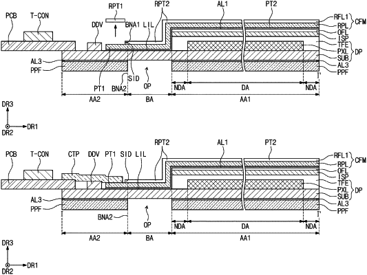
preparing a display panel that comprises:
a first area;
a bending area extending from the first area; and
a second area extending from the bending area;
attaching an anti-reflection layer to the display panel;
removing a first removal section of a first releasing film disposed on the anti-reflection layer, the first removal section overlapping the second area of the display panel in a plan view;
providing a cover tape onto a first section of the anti-reflection layer that overlaps the second area of the display panel in a plan view; and
removing a second removal section of the first releasing film that overlaps both the first area and the bending area of the display panel in a plan view.
|