US 11,812,646 B2
Display device and manufacturing method thereof
Sheng-Yu Wu, Hsinchu (TW); Mirng-Ji Lii, Hsinchu County (TW); Shang-Yun Tu, Hsinchu (TW); and Ching-Hui Chen, Hsinchu (TW)
Assigned to Taiwan Semiconductor Manufacturing Company, Ltd., Hsinchu (TW)
Filed by Taiwan Semiconductor Manufacturing Company, Ltd., Hsinchu (TW)
Filed on Jan. 21, 2022, as Appl. No. 17/580,659.
Application 17/580,659 is a continuation of application No. 16/866,519, filed on May 4, 2020, granted, now 11,239,305.
Claims priority of provisional application 62/877,846, filed on Jul. 24, 2019.
Prior Publication US 2022/0149141 A1, May 12, 2022
This patent is subject to a terminal disclaimer.
Int. Cl. H01L 21/00 (2006.01); H10K 59/131 (2023.01); H10K 59/121 (2023.01); H10K 71/00 (2023.01)
CPC H10K 59/131 (2023.02) [H10K 59/121 (2023.02); H10K 71/00 (2023.02)] 20 Claims
OG exemplary drawing
 
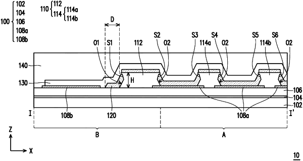
1. A display device, comprising:
a semiconductor substrate having a pixel region and a peripheral region located around the pixel region, wherein the semiconductor substrate includes first electrodes disposed in the pixel region;
a first isolation pattern disposed in the peripheral region of the semiconductor substrate, wherein the first isolation pattern has a first side surface facing away from the pixel region;
a light-emitting layer disposed on the first isolation pattern and the first electrodes, and covering the first side surface of the first isolation pattern; and
a second electrode disposed on the light-emitting layer.