| CPC H10K 59/124 (2023.02) [H10K 59/122 (2023.02); H10K 59/123 (2023.02); H10K 59/1213 (2023.02); H10K 59/1216 (2023.02); H10K 59/131 (2023.02); H10K 59/352 (2023.02); H10K 71/00 (2023.02); H01L 27/124 (2013.01); H01L 27/1248 (2013.01); H01L 27/1255 (2013.01); H01L 27/1259 (2013.01); H10K 59/1201 (2023.02)] | 17 Claims |
|
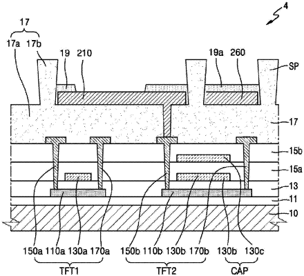
1. A display apparatus comprising:
a thin film transistor disposed on a substrate;
a first insulating layer having a single-layered structure and covering the thin film transistor in a first direction, wherein the first insulating layer includes a first portion having a first thickness, in the first direction, and a second potion having a second thickness, in the first direction, that is less than the first thickness;
a pixel electrode disposed on the second portion of the first insulating layer, in the first direction, surrounded by the first portion, in a second direction different from the first direction,
wherein the pixel electrode is electrically connected to the thin film transistor;
a pixel defining layer disposed on an edge of the pixel electrode;
a signal line on the second portion of the first insulating layer, in the first directions
wherein the signal line and the pixel electrode are spaced apart from each other in the second direction and include substantially the same material; and
a second insulating layer completely covering the signal line in the first direction, wherein the second insulating layer and the pixel defining layer include substantially the same material.
|