| CPC H05K 1/189 (2013.01) [H05K 7/20963 (2013.01); H05K 9/0054 (2013.01); G06F 3/044 (2013.01); H05K 1/147 (2013.01); H05K 9/009 (2013.01); H05K 9/0081 (2013.01); H05K 2201/056 (2013.01); H05K 2201/10128 (2013.01); H05K 2201/10136 (2013.01)] | 19 Claims |
|
1. A display device, comprising:
a display panel;
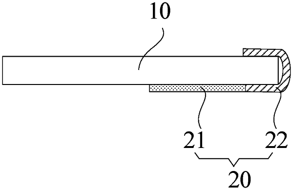
a circuit board, one end of the circuit board being connected to the display panel, the circuit board being at least partially disposed on a back surface of the display panel and comprising a device region on a side distal from the display panel;
at least one electronic device disposed in the device region; and
an adhesive tape disposed on the side distal from the display panel of the circuit board and bonded to a back surface of at least one part of the circuit board and the back surface of the display panel; wherein
at least one part of the at least one electronic device in the device region is disposed between the adhesive tape and the back surface of the display panel;
wherein the adhesive tape comprises a first insulating layer, a functional layer, and a second insulating layer that are sequentially laminated; wherein the first insulating layer is bonded to the at least one part of the circuit board and at least one part of the display panel, and the functional layer comprises at least one of an electromagnetic shielding layer, an electromagnetic wave absorbing layer, and a heat dissipating layer.
|