| CPC H05K 1/187 (2013.01) [H05K 1/147 (2013.01); H05K 3/0097 (2013.01); H05K 3/284 (2013.01); H05K 2201/09754 (2013.01); H05K 2201/10106 (2013.01); H05K 2201/10151 (2013.01)] | 20 Claims |
|
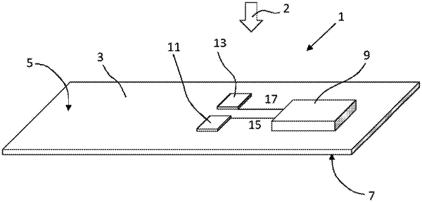
1. A method of making an electrical device comprising:
(i) providing a layer of interlayer material having a first major surface and a second opposing major surface;
(ii) positioning at least a first electrically operable component on the first major surface of the first layer of interlayer material, the first electrically operable component being mounted on a first circuit board; and
(iii) providing a layer of adhesive material to cover at least a portion of the first major surface of the layer of interlayer material and at least a portion of the first electrically operable component and/or at least a portion of the first circuit board
such that following (iii) the first electrically operable component is fixed on the layer of interlayer material by at least a portion of the layer of adhesive material,
wherein following (ii) at least a second electrically operable component is positioned on the layer of interlayer material, the second electrically operable component being mounted on a second circuit board, further wherein the second electrically operable component is spaced apart from the first electrically operable device and/or the first circuit board is spaced apart from the second circuit board.
|