| CPC H05K 1/185 (2013.01) [H05K 3/4682 (2013.01); H05K 2201/0195 (2013.01); H05K 2203/1469 (2013.01)] | 8 Claims |
|
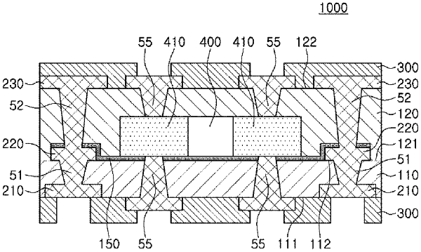
1. A printed circuit board comprising:
a first insulating layer;
a first circuit pattern, disposed on one surface of the first insulating layer, enclosed in the first insulating layer in such a way that one surface of the first circuit pattern is exposed through the one surface of the first insulating layer and remaining surfaces of the first circuit pattern excluding the one surface of the first circuit pattern are covered by the first insulating layer;
a second circuit pattern, disposed on second surface of the first insulating layer, spaced apart from the first circuit pattern and protruded from the second surface of the first insulating layer toward an opposite side of the first circuit pattern;
an adhesive layer disposed on the second surface of the first insulating layer to contact a portion of the first insulating layer and a side surface of the second circuit pattern;
an electronic component disposed on the adhesive layer and adjacent to the second circuit pattern such that the electronic component at least partially overlaps the second circuit pattern along a direction normal to a thickness direction of the printed circuit board;
a second insulating layer disposed on the second surface of the first insulating layer and covering at least a portion of each of the electronic component and the second circuit pattern;
a first via formed in the first insulating layer and connecting the second circuit pattern to the first circuit pattern;
a second via formed in the second insulating layer and connecting the second circuit pattern to a third circuit pattern disposed on one surface of the second insulating layer;
and a third via formed in the first insulating layer and connected to the electronic component,
wherein a height of the second via is greater than a height of the first via,
wherein the first via and the second via have shapes tapered in same directions to each other, and
wherein the second via and the third via have shapes tapered in opposite directions to each other.
|