| CPC H05K 1/144 (2013.01) [H01Q 1/243 (2013.01); H04M 1/0264 (2013.01); H04M 1/0277 (2013.01); H05K 1/025 (2013.01); H05K 1/0243 (2013.01); H05K 1/0366 (2013.01); H05K 1/115 (2013.01); H05K 3/4644 (2013.01); H05K 5/0086 (2013.01); H04M 1/03 (2013.01); H05K 2201/042 (2013.01); H05K 2201/09027 (2013.01); H05K 2201/1009 (2013.01); H05K 2201/10098 (2013.01); H05K 2201/10121 (2013.01); H05K 2201/10151 (2013.01); H05K 2201/10234 (2013.01)] | 14 Claims |
|
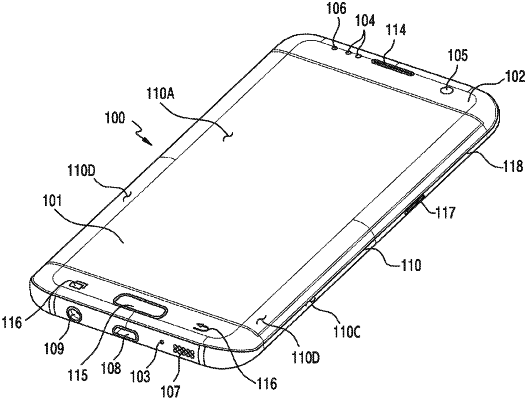
1. An electronic device comprising:
a support member;
a display disposed at a first side of the support member;
a battery disposed at a second side of the support member opposite to the display;
a first printed circuit board (PCB) disposed at the second side of the support member; and
a second PCB,
wherein the first PCB includes one area having a first width in a first direction and another area having a second width in the first direction, the second width being smaller than the first width,
wherein, in the first direction, the another area is disposed between an edge of the battery and an edge of the electronic device,
wherein the second width is reduced from the first width by at least a width of the battery,
wherein the battery and the another area of the first PCB are disposed adjacent in the first direction such that the battery and the first PCB do not overlap,
wherein the first PCB includes a first electrical terminal and a second electrical terminal,
wherein the second PCB is stacked with another area of the first PCB to overlap the first electrical terminal and the second electrical terminal and is electrically connected to the first electrical terminal and the second electrical terminal, and
wherein the second PCB includes a line connecting the first electrical terminal and the second electrical terminal such that current from the first PCB is provided to the second PCB via the first electrical terminal and the current is provided from the second PCB to the second electrical terminal of the first PCB via the line of the second PCB.
|