| CPC H04B 10/2971 (2013.01) [H04J 14/0216 (2013.01); H04Q 11/0005 (2013.01)] | 22 Claims |
|
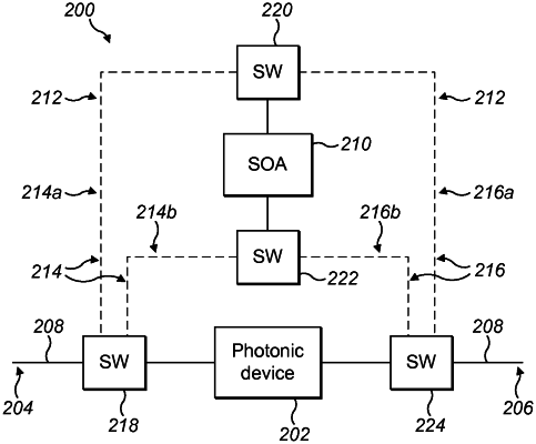
1. A device for processing an optical signal, the device comprising:
a photonic device arranged between a first input/output and a second input/output, the photonic device being in optical communication with the first and second inputs/outputs by a signal path, the signal path being selectively for transmission of a first optical signal in a first direction from the first input/output to the second input/output and for transmission of a second optical signal in a second direction from the second input/output to the first input/output;
an optical gain element for receiving the first or second optical signal and outputting an amplified first or second optical signal respectively, the optical gain element being selectively configurable to optically amplify the first optical signal downstream of the photonic device in the first direction and the second optical signal downstream of the photonic device in the second direction; and
a path switching circuit comprising:
a first signal amplification path connectable between the first input/output and the photonic device for optically coupling the signal path to and from the optical gain element, the first optical signal being transmitted through the photonic device in the first direction;
a second signal amplification path connectable between the photonic device and the second input/output for optically coupling the signal path to and from the optical gain element, the second optical signal being transmitted through the photonic device in the second direction; and
the path switching circuit being configured to selectively connect the first signal amplification path and the second signal amplification path into the signal path.
|