| CPC H04B 1/40 (2013.01) [H03F 3/19 (2013.01); H03F 2200/294 (2013.01); H03F 2200/451 (2013.01)] | 19 Claims |
|
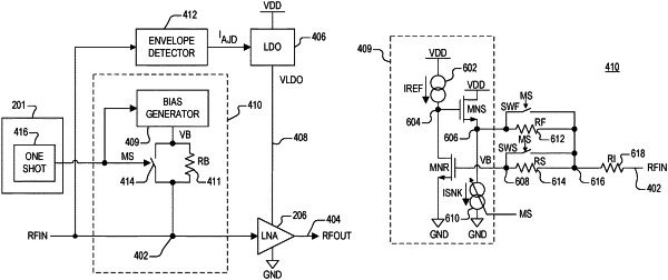
1. A bias circuit for a low noise amplifier of a front end interface of a radio frequency communication device, the bias circuit comprising:
a bias generator that provides a bias voltage on a bias node for the low noise amplifier, wherein a current capacity of the bias generator is at a default level for each of a plurality of modes;
a first resistive device coupled between the bias node and an input of the low noise amplifier;
a first switch coupled in parallel with the first resistive device; and
mode control circuitry receiving at least one mode signal indicative of a mode change from a first one of the plurality of modes to a second one of the plurality of modes, wherein the mode control circuitry, in response to a mode change, momentarily activates the first switch to bypass the first resistive device and momentarily increases current capacity of the bias generator from the default level by momentarily increasing its capacity to sink current before returning the current capacity back to the default level for the second one of the plurality of modes.
|