| CPC H03K 3/012 (2013.01) [G11C 7/10 (2013.01); G11C 7/222 (2013.01); H03K 3/0372 (2013.01)] | 20 Claims |
|
1. A latch circuit, comprising:
a latch clock generator configured to generate a latched clock signal based on a clock signal and a first enable signal; and
an input latch coupled to the latch clock generator to receive the latched clock signal, the input latch configured to generate a latched output signal based on the latched clock signal and an input signal,
wherein, in response to the first enable signal having a disabling logic level, the latch clock generator is configured to set a logic level of the latched clock signal to a corresponding disabling logic level, regardless of the clock signal,
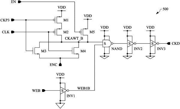
wherein the latch clock generator comprises: a NAND gate and a transistor,
wherein the NAND gate comprises:
a first input configured to receive a signal corresponding to the first enable signal,
a second input coupled to an internal node to receive an internal clock signal corresponding to the clock signal, and
an output at which the NAND gate is configured to output the latched clock signal, and
wherein the transistor comprises:
a first terminal coupled to a node of a power supply voltage,
a second terminal coupled to the internal node, and
a gate terminal configured to receive a second enable signal.
|