| CPC H03H 9/174 (2013.01) [H03H 3/02 (2013.01); H03H 9/02015 (2013.01); H03H 9/02031 (2013.01); H03H 9/02228 (2013.01); H03H 9/132 (2013.01); H03H 9/176 (2013.01); H03H 9/205 (2013.01); H03H 9/547 (2013.01); H03H 9/562 (2013.01); H03H 9/564 (2013.01); H03H 9/568 (2013.01); H10N 30/06 (2023.02); H03H 2003/023 (2013.01); Y10T 29/42 (2015.01); Y10T 29/49005 (2015.01)] | 9 Claims |
|
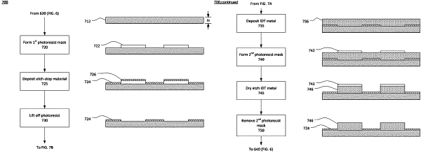
1. A method of fabricating an acoustic resonator device comprising:
forming a patterned first photoresist mask on a front surface of a single-crystal piezoelectric plate at locations of a desired IDT pattern;
blanket depositing an etch-stop layer on the front surface of the single-crystal piezoelectric plate where the patterned first photoresist mask does not exist and on the patterned first photoresist mask;
removing the patterned first photoresist mask and the etch-stop layer on the patterned first photoresist mask to expose the front surface of the piezoelectric plate at locations of the desired IDT pattern;
blanket depositing a conductor material on the etch stop layer and on the exposed front surface of the piezoelectric plate;
forming a patterned second photoresist mask on the conductor material at locations of the desired IDT pattern;
using an etch process to remove portions of the conductor material over and to the etch-stop layer to form an interdigital transducer (IDT) with the desired IDT pattern, the desired IDT pattern having interleaved fingers disposed on a diaphragm configured to span a cavity in a substrate supporting the piezoelectric plate, a portion of the piezoelectric plate and the etch-stop layer forming the diaphragm, wherein the etch-stop layer and the second photoresist mask are impervious to the etch process; and
removing the patterned second photoresist mask from the IDT to leave the IDT with the desired IDT pattern.
|