US 11,811,367 B2
Scalable periphery tunable matching power amplifier
Dan William Nobbe, Crystal Lake, IL (US); David Halchin, Summerfield, NC (US); Jeffrey A. Dykstra, Woodstock, IL (US); Michael P. Gaynor, Crystal Lake, IL (US); David Kovac, Arlington Heights, IL (US); Kelly Michael Mekechuk, Austin, TX (US); Gary Frederick Kaatz, Barrington, IL (US); and Chris Olson, Palatine, IL (US)
Assigned to pSemi Corporation, San Diego, CA (US)
Filed by pSemi Corporation, San Diego, CA (US)
Filed on Apr. 27, 2022, as Appl. No. 17/731,048.
Application 17/731,048 is a continuation of application No. 16/987,097, filed on Aug. 6, 2020, granted, now 11,323,078.
Application 16/987,097 is a continuation of application No. 16/408,001, filed on May 9, 2019, granted, now 10,756,684, issued on Aug. 25, 2020.
Application 16/408,001 is a continuation of application No. 15/827,984, filed on Nov. 30, 2017, granted, now 10,333,471, issued on Jun. 25, 2019.
Application 15/827,984 is a continuation of application No. 14/957,399, filed on Dec. 2, 2015, granted, now 9,847,759, issued on Dec. 19, 2017.
Application 14/957,399 is a continuation of application No. 13/797,779, filed on Mar. 12, 2013, granted, now 9,294,056, issued on Mar. 22, 2016.
Prior Publication US 2022/0329215 A1, Oct. 13, 2022
This patent is subject to a terminal disclaimer.
Int. Cl. H03F 1/56 (2006.01); H03F 3/21 (2006.01); H03F 1/02 (2006.01); H03F 1/22 (2006.01); H03F 3/195 (2006.01); H03F 3/24 (2006.01); H03F 3/72 (2006.01); H03F 3/217 (2006.01); H03F 3/193 (2006.01)
CPC H03F 1/56 (2013.01) [H03F 1/0205 (2013.01); H03F 1/0261 (2013.01); H03F 1/0277 (2013.01); H03F 1/223 (2013.01); H03F 3/193 (2013.01); H03F 3/195 (2013.01); H03F 3/211 (2013.01); H03F 3/2176 (2013.01); H03F 3/245 (2013.01); H03F 3/72 (2013.01); H03F 2200/108 (2013.01); H03F 2200/222 (2013.01); H03F 2200/27 (2013.01); H03F 2200/387 (2013.01); H03F 2200/411 (2013.01); H03F 2200/432 (2013.01); H03F 2200/451 (2013.01); H03F 2203/21109 (2013.01); H03F 2203/7215 (2013.01); H03F 2203/7221 (2013.01)] 20 Claims
OG exemplary drawing
 
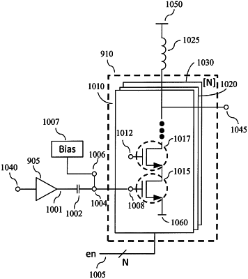
1. An amplification circuit, comprising:
one or more amplifiers configured to be selectively activated or deactivated,
wherein each amplifier of the one or more amplifiers comprises:
a stack of a plurality of transistors, and
one or more non-bypassing gate capacitors connected to respective one or more transistors of the plurality of transistors;
wherein, in each amplifier:
an input transistor of the plurality of transistors is configured to receive an input signal through a single common input coupling capacitor, the single common input coupling capacitor being common among the one or more amplifiers,
and
the one or more non-bypassing gate capacitors are configured to allow one or more first radio frequency (RF) gate voltages of respective one or more transistors of the plurality of transistors to vary along with one or more second RF voltages at one or more sources of the respective one or more transistors of the plurality of transistors.