| CPC H02M 3/1582 (2013.01) [H02M 1/0054 (2021.05); H02M 1/0058 (2021.05)] | 17 Claims |
|
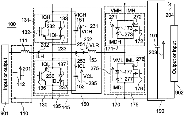
1. A bidirectional boost or buck power converter for converting an input primary power having an input primary voltage and an input primary current into an output secondary power having an output secondary voltage and output secondary current or an input secondary power having an input secondary voltage and an input secondary current into an output primary power having an output primary voltage and second primary current respectively; the power converter including at least one:
primary switching arrangement comprising at least one primary switching unit having a primary dynamical switching loss;
secondary switching arrangement comprising at least one secondary switching unit having a secondary dynamical switching loss; and,
resonant unit connecting the at least one primary switching unit and the at least one secondary switching unit;
the primary switching arrangement comprising at least a first primary switching unit including a first primary transistor and a first primary diode and a second primary switching unit including a second primary transistor and a second primary diode;
the at least first primary switching unit being series connected to the second primary switching unit;
the secondary switching arrangement comprising at least a first secondary switching unit including a first secondary transistor and a first secondary diode and a second secondary switching unit including a second secondary transistor and a second secondary diode;
the at least first secondary switching unit being series connected to the second secondary switching unit;
the resonant unit comprising an inductor and a first capacitor connecting a primary terminal and a secondary terminal, and a second capacitor connecting the primary terminal and a common terminal;
the resonant unit having a natural frequency defined as a reciprocal of a product of the inductor by a sum of the first capacitor and second capacitor;
a dimension of a component of the primary switching arrangement being larger than a dimension of a component of the secondary switching arrangement, such that the primary switching arrangement dissipates more heat than the secondary switching arrangement;
the primary dynamical switching loss being higher than the secondary dynamical switching loss;
the first primary transistor, the second primary transistor, the first secondary transistor, and the second secondary transistor having each a periodic control signal;
the periodic control signal having a rising edge and a falling edge on each period of the periodic control signal;
the falling edge of the periodic control signal of the second secondary transistor and the rising edge of the periodic control signal of the second primary transistor having a first time delay during which the first primary transistor, the second primary transistor, the first secondary transistor, and the second secondary transistor are all turned OFF;
the first time delay being equal to a third of a ratio of pi to the natural frequency;
the falling edge of the periodic control signal of the first secondary transistor and the rising edge of the periodic control signal of the first primary transistor having a second time delay, during which the first primary transistor, the second primary transistor, the first secondary transistor, and the second secondary transistor are all turned OFF;
the second time delay being equal to a third of a ratio of pi to the natural frequency;
the falling edge of the periodic control signal of the second primary transistor and the rising edge of the periodic control signal of the first secondary transistor having a third time delay during which the first primary transistor, the second primary transistor, the first secondary transistor, and the second secondary transistor are all turned OFF;
the third time delay being dependent on the primary switching unit technology;
the falling edge of the periodic control signal of the first primary transistor and the rising edge of the periodic control signal of the second secondary transistor having a fourth time delay during which the first primary transistor, the second primary transistor, the first secondary transistor, and the second secondary transistor are all turned OFF;
the fourth time delay being dependent on the primary switching unit technology;
the primary switching arrangement being connected to the primary terminal, the secondary terminal, and the common terminal;
the secondary switching arrangement being connected to the secondary terminal and to the common terminal; and
the primary switching arrangement being electrically connected to the secondary switching arrangement in a continuous current mode via the secondary terminal and the common terminal.
|