US 11,811,312 B2
Charge pump circuit
John P. Lesso, Edinburgh (GB); Peter J. Frith, Edinburgh (GB); and John L. Pennock, Edinburgh (GB)
Assigned to Cirrus Logic, Inc., Austin, TX (US)
Filed by Cirrus Logic International Semiconductor Ltd., Edinburgh (GB)
Filed on Jun. 21, 2022, as Appl. No. 17/845,007.
Application 17/845,007 is a continuation of application No. 17/347,151, filed on Jun. 14, 2021, granted, now 11,398,777.
Application 17/347,151 is a continuation of application No. 16/988,796, filed on Aug. 10, 2020, granted, now 11,043,894.
Application 16/988,796 is a continuation of application No. 16/450,129, filed on Jun. 24, 2019, granted, now 10,819,229.
Application 16/450,129 is a continuation of application No. 16/023,114, filed on Jun. 29, 2018, granted, now 10,333,395.
Application 16/023,114 is a continuation of application No. 15/597,850, filed on May 17, 2017, granted, now 10,014,769.
Application 15/597,850 is a continuation of application No. 15/205,439, filed on Jul. 8, 2016, granted, now 9,685,856.
Application 15/205,439 is a continuation of application No. 14/542,086, filed on Nov. 14, 2014, granted, now 9,391,508.
Application 14/542,086 is a continuation of application No. 13/403,450, filed on Feb. 23, 2012, granted, now 8,890,604.
Application 13/403,450 is a continuation of application No. 13/336,795, filed on Dec. 23, 2011, abandoned.
Claims priority of provisional application 61/427,431, filed on Dec. 27, 2010.
Claims priority of application No. 1021810 (GB), filed on Dec. 23, 2010.
Prior Publication US 2022/0321003 A1, Oct. 6, 2022
This patent is subject to a terminal disclaimer.
Int. Cl. H02M 3/07 (2006.01); H03F 3/181 (2006.01); H02M 1/00 (2006.01)
CPC H02M 3/07 (2013.01) [H02M 1/00 (2013.01); H02M 3/072 (2021.05); H03F 3/181 (2013.01); H02M 1/009 (2021.05); H02M 1/0083 (2021.05); H02M 3/071 (2021.05)] 20 Claims
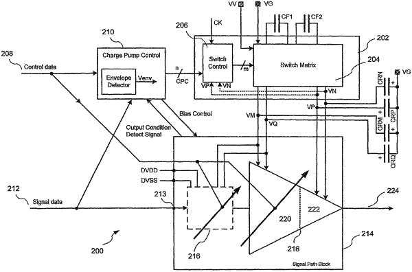
OG exemplary drawing
 
1. A battery-powered device comprising:
a charge pump circuit comprising:
an input node and a reference node for connection to an input voltage, a first pair of output nodes and a second pair of output nodes and two pairs of flying capacitor nodes;
a network of switching paths for interconnecting said nodes; and
a controller configured to control the network of switching paths when in use with two flying capacitors connected to the two pairs of flying capacitor nodes, to provide a first bipolar output voltage at the first pair of output nodes and a second bipolar output voltage at the second pair of bipolar output nodes.