| CPC H02K 11/33 (2016.01) [B64D 27/24 (2013.01); H01L 23/3121 (2013.01); H01L 23/3735 (2013.01); H01L 23/5383 (2013.01); H01L 23/5386 (2013.01); H01L 25/16 (2013.01); H05K 1/0209 (2013.01); B64D 27/10 (2013.01); B64D 2027/026 (2013.01); H02K 2211/03 (2013.01)] | 21 Claims |
|
1. A power electronics converter comprising:
a multi-layer planar carrier substrate comprising a plurality of electrically conductive layers;
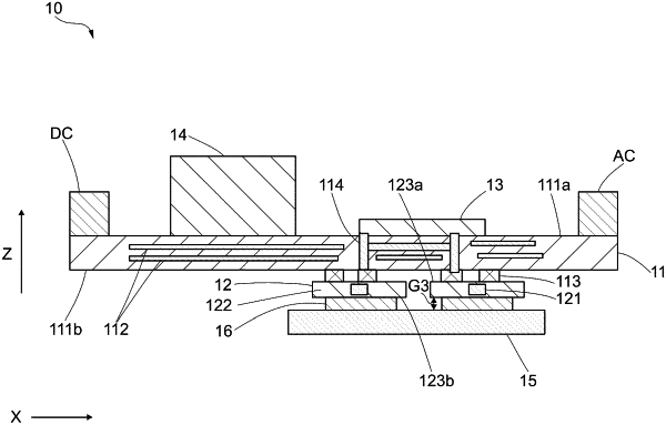
a converter commutation cell comprising a power circuit and a gate driver circuit, the power circuit comprising at least one power semiconductor switching element and at least one capacitor, wherein each power semiconductor switching element of the at least one power semiconductor switching element is comprised in a power semiconductor prepackage, each power semiconductor prepackage comprising one or more power semiconductor switching elements embedded in a solid insulating material, and at least one electrical connection extending in a direction from at least one terminal of each of the one or more power semiconductor switching elements through the solid insulating material directly to an electrical connection side of the respective power semiconductor prepackage, at least one of the terminals of each of the one or more power semiconductor switching elements of the respective semiconductor prepackage being connected to at least one conductive layer of the plurality of electrically conductive layers of the multi-layer planar carrier substrate at the electrical connection side of the respective power semiconductor prepackage;
a heat sink arranged to remove heat from the respective power semiconductor prepackage at a heat removal side of the respective power semiconductor prepackage, the heat removal side being opposite the electrical connection side; and
a thermal interface layer arranged between the heat removal side of the respective power semiconductor prepackage and the heat sink, the thermal interface layer having a thermal conductivity and a mechanical compressibility,
wherein a converter parameter Ω satisfies 0.1 MNK/Wm<Ω<1 GNK/Wm, the converter parameter Ω being defined as the mechanical compressibility of the thermal interface layer divided by the thermal conductivity of the thermal interface layer.
|