US 11,811,133 B2
Electronic device antenna arrays mounted against a dielectric layer
Jennifer M. Edwards, San Francisco, CA (US); Harish Rajagopalan, San Jose, CA (US); Simone Paulotto, Redwood City, CA (US); Bilgehan Avser, San Bruno, CA (US); Hao Xu, Cupertino, CA (US); Rodney A. Gomez Angulo, Santa Clara, CA (US); Siwen Yong, Mountain View, CA (US); Matthew A. Mow, Los Altos, CA (US); and Mattia Pascolini, San Francisco, CA (US)
Assigned to Apple Inc., Cupertino, CA (US)
Filed by Apple Inc., Cupertino, CA (US)
Filed on May 7, 2021, as Appl. No. 17/314,740.
Application 17/314,740 is a continuation of application No. 15/950,677, filed on Apr. 11, 2018, granted, now 11,139,588.
Prior Publication US 2021/0265745 A1, Aug. 26, 2021
This patent is subject to a terminal disclaimer.
Int. Cl. H01Q 1/24 (2006.01); H01Q 3/26 (2006.01); H01Q 9/04 (2006.01); H01Q 21/06 (2006.01); H01Q 21/22 (2006.01); H01Q 1/38 (2006.01)
CPC H01Q 1/243 (2013.01) [H01Q 1/38 (2013.01); H01Q 3/26 (2013.01); H01Q 3/2605 (2013.01); H01Q 3/2658 (2013.01); H01Q 21/061 (2013.01); H01Q 21/065 (2013.01); H01Q 21/22 (2013.01)] 19 Claims
OG exemplary drawing
 
1. An electronic device comprising:
a housing comprising peripheral conductive housing sidewalls and a dielectric housing layer coupled to the peripheral conductive housing sidewalls;
a dielectric substrate having a surface that is mounted against the dielectric housing layer; and
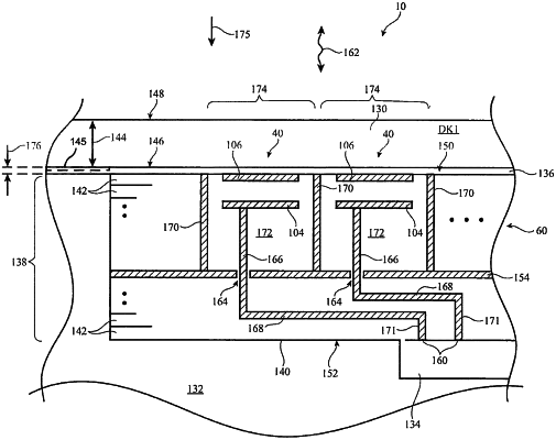
a phased antenna array having parasitic elements at the surface of the dielectric substrate and antenna resonating elements overlapping the parasitic elements, wherein the phased antenna array is configured to convey radio-frequency signals at a frequency between 10 GHz and 300 GHz through the dielectric housing layer.