| CPC H01P 1/184 (2013.01) [H01P 1/181 (2013.01); H01P 11/003 (2013.01)] | 18 Claims |
|
1. A manufacture method for manufacturing a phase shifter, comprising:
providing a dielectric substrate; and
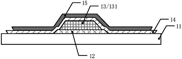
forming a transmission line, a dielectric layer, an insulating layer, and a metal layer disposed with respect to the dielectric substrate,
wherein in a direction perpendicular to a first surface of the dielectric substrate, the dielectric layer and the insulating layer are between the metal layer and the transmission line, a material of the dielectric layer is a semiconductor material, and
an orthographic projection of the metal layer on the dielectric substrate, an orthographic projection of the insulating layer on the dielectric substrate, and an orthographic projection of the dielectric layer on the dielectric substrate at least partially overlap;
wherein forming the transmission line, the dielectric layer, the insulating layer, and the metal layer disposed with respect to the dielectric substrate, comprises:
forming the transmission line on the first surface of the dielectric substrate;
forming the dielectric layer on a side of the transmission line away from the dielectric substrate;
forming the insulating layer on the dielectric substrate on which the dielectric layer is formed, wherein the insulating layer is formed on a side of the dielectric layer away from the dielectric substrate; and
forming the metal layer on a side of the insulating layer away from the dielectric substrate.
|