| CPC H01L 33/62 (2013.01) [H01L 27/156 (2013.01); H01L 33/22 (2013.01); H01L 33/382 (2013.01); H01L 33/46 (2013.01); H01L 33/50 (2013.01); H01L 33/58 (2013.01); H01L 33/642 (2013.01); F21K 9/23 (2016.08); F21K 9/27 (2016.08); H01L 2933/0016 (2013.01); H01L 2933/0025 (2013.01); H01L 2933/0041 (2013.01); H01L 2933/0066 (2013.01)] | 20 Claims |
|
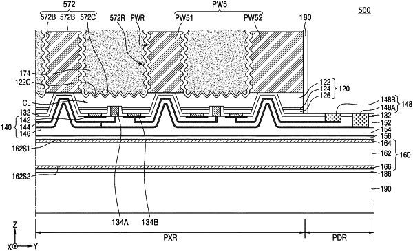
1. A light source module comprising:
a light-emitting cell;
a wiring structure provided on the light-emitting cell and connected to the light-emitting cell;
a support substrate that is apart from the light-emitting cell with the wiring structure provided between the support substrate and the light-emitting cell in a vertical direction;
a printed circuit board that is apart from the wiring structure with the support substrate provided between the printed circuit board and the wiring structure in the vertical direction, the printed circuit board overlapping the light-emitting cell in the vertical direction, and the printed circuit board being adhered onto the support substrate; and
at least one insulating film that is apart from the wiring structure in the vertical direction, the at least one insulating film covering at least one of a first surface of the support substrate, which faces the wiring structure, and a second surface of the support substrate, which faces the printed circuit board.
|