US 11,810,995 B2
P-type doping in GaN LEDs for high speed operation at low current densities
Bardia Pezeshki, Mountain View, CA (US); and Cameron Danesh, Mountain View, CA (US)
Assigned to AvicenaTech Corp., Mountain View, CA (US)
Filed by AvicenaTech Corp., Sunnyvale, CA (US)
Filed on Dec. 3, 2021, as Appl. No. 17/542,201.
Claims priority of provisional application 63/121,091, filed on Dec. 3, 2020.
Prior Publication US 2022/0181517 A1, Jun. 9, 2022
Int. Cl. H04B 10/04 (2006.01); H01L 33/06 (2010.01); H01L 33/02 (2010.01); H04B 10/25 (2013.01); H04B 10/61 (2013.01); H01L 33/32 (2010.01)
CPC H01L 33/06 (2013.01) [H01L 33/025 (2013.01); H01L 33/325 (2013.01); H04B 10/25 (2013.01); H04B 10/615 (2013.01)] 10 Claims
OG exemplary drawing
 
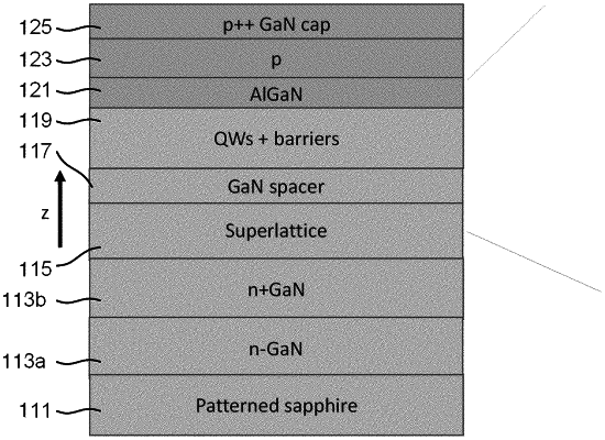
1. An LED comprising:
a p type GaN layer;
an n type GaN layer; and
a plurality of alternating quantum well layers and barrier layers between the p type GaN layer and the n type GaN layer, with the quantum well layers being undoped and with the barrier layers being p-doped with Mg having a doping concentration of at least 1019/cm3, but only in a central portion of each barrier layer.