| CPC H01L 31/109 (2013.01) [H01L 31/022408 (2013.01); H01L 31/1016 (2013.01); H01L 31/1868 (2013.01)] | 9 Claims |
|
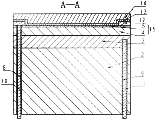
1. An infrared-transmitting high-sensitivity visible light detector, characterized in that it comprises an intrinsic monocrystalline silicon substrate, a lower electrode, a heterojunction for detecting visible light, a metal frame, an upper electrode and a passivation layer from bottom to top; wherein the heterojunction comprises a heterojunction lower layer and a heterojunction upper layer;
the upper electrode is made of conductive and transparent material to visible light and infrared, which is a grid composed of one-dimensional conductive nanowires; the heterojunction upper layer is a nano-film sensitive to visible light and transparent to infrared; the heterojunction lower layer is intrinsic monocrystalline silicon; the lower electrode is a conductive layer formed by heavily doped ions of intrinsic monocrystalline silicon; below the lower electrode is an intrinsic monocrystalline silicon substrate;
characterized in that the metal frame is square and annular and surrounds the upper electrode from all sides; the upper electrode is step-shaped and comprises peripheral step, a middle bottom and side walls connecting the peripheral steps and the middle bottom, wherein the peripheral step of the upper electrode is higher than the middle bottom; the upper surface of the metal frame is in contact with the lower surface of the peripheral step of the upper electrode, the inside of the metal frame is in contact with the side walls of the upper electrode, and the lower surface of the metal frame is in contact with the heterojunction upper layer, the lower surface of the middle bottom of the upper electrode is in contact with the upper surface of the heterojunction upper layer.
|