| CPC H01L 31/02363 (2013.01) [G01T 1/20183 (2020.05); G01T 1/24 (2013.01); H01L 27/1461 (2013.01); H01L 27/14676 (2013.01); H01L 31/115 (2013.01)] | 20 Claims |
|
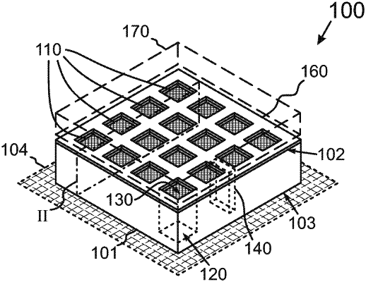
1. A radiation sensor element comprising a semiconductor substrate, having bulk majority charge carriers of a first polarity, a bulk refractive index, a front surface, defining a front side of the semiconductor substrate, and a back surface, arranged opposite the front surface and extending substantially along a base plane;
the radiation sensor element comprising a plurality of pixel portions, each pixel portion of the plurality of pixel portions comprising a collection region on the back surface for collecting free charge carriers of a second polarity opposite in sign to the first polarity;
wherein each pixel portion of the plurality of pixel portions comprises a textured region on the front surface, the textured region comprising high aspect ratio nanostructures, extending substantially along a thickness direction perpendicular to the base plane and forming an optical conversion layer, having an effective refractive index gradually changing towards the bulk refractive index to reduce reflection of light emitted by a scintillator and incident on said pixel portion from the front side of the semiconductor substrate;
the radiation sensor element comprises an intermediate portion between two pixel portions of the plurality of pixel portions, the intermediate portion comprising an intermediate region on the front surface with a root mean square, RMS, roughness lower than a RMS roughness of a textured region of either of the two pixel portions; and
the radiation sensor element comprises the scintillator coupled to the intermediate region.
|