| CPC H01L 29/78696 (2013.01) [H01L 21/76829 (2013.01); H01L 27/0688 (2013.01); H01L 27/1259 (2013.01); H01L 29/6675 (2013.01); H01L 29/78618 (2013.01)] | 21 Claims |
|
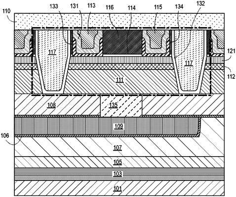
1. A semiconductor device, comprising:
a substrate;
a transistor above the substrate, wherein the transistor includes a channel layer above the substrate, and wherein the channel layer includes:
a first channel material of a first conductivity;
elements of one or more additional materials distributed within the channel layer, wherein the channel layer including the elements of the one or more additional materials has a second conductivity different from the first conductivity;
a capping layer on the first channel material; and
a spacer on the capping layer, the spacer and the capping layer having a same lateral width.
|