US 11,810,978 B2
Gate resistance improvement and method thereof
Ju-Li Huang, Nantou County (TW); Hsin-Che Chiang, Taipei (TW); Yu-Chi Pan, Zhubei (TW); Chun-Ming Yang, Taipei (TW); Chun-Sheng Liang, Changhua County (TW); Ying-Liang Chuang, Zhubei (TW); and Ming-Hsi Yeh, Hsinchu (TW)
Assigned to Taiwan Semiconductor Manufacturing Co., Ltd., Hsinchu (TW)
Filed by Taiwan Semiconductor Manufacturing Co., Ltd., Hsinchu (TW)
Filed on Jun. 4, 2021, as Appl. No. 17/339,020.
Application 17/339,020 is a division of application No. 16/287,368, filed on Feb. 27, 2019, granted, now 11,031,500.
Claims priority of provisional application 62/712,394, filed on Jul. 31, 2018.
Prior Publication US 2021/0296483 A1, Sep. 23, 2021
Int. Cl. H01L 29/78 (2006.01); H01L 29/423 (2006.01); H01L 21/285 (2006.01); H01L 29/40 (2006.01); H01L 21/3213 (2006.01); H01L 29/49 (2006.01)
CPC H01L 29/785 (2013.01) [H01L 21/28556 (2013.01); H01L 21/32134 (2013.01); H01L 29/401 (2013.01); H01L 29/42372 (2013.01); H01L 29/4966 (2013.01)] 20 Claims
OG exemplary drawing
 
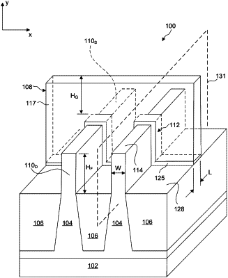
1. A fin field-effect transistor (finFET) device, comprising:
a substrate;
a fin over the substrate; and
a gate structure over the fin and having a first top surface, the gate structure comprising:
a work-function metal (WFM) layer over an inner sidewall of the gate structure and having a second top surface lower than the first top surface;
a filler gate metal layer over the second top surface of the WFM layer and having a third top surface substantially co-planar with the first top surface; and
a self-assembled monolayer (SAM) in physical contact with the filler gate metal layer and the WFM layer.