| CPC H01L 29/7813 (2013.01) [H01L 29/4236 (2013.01)] | 24 Claims |

|
1. A semiconductor device comprising:
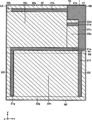
a semiconductor layer including a first plane extending along a plane including a first axis and a second axis;
a first electrode extending along the first axis;
a second electrode extending along the second axis;
a third electrode extending along the first axis;
a fourth electrode extending along the second axis; and
a fifth electrode above the first plane, the fifth electrode being electrically coupled to the first electrode and the second electrode, and including a first portion, a second portion, a third portion, the first portion crossing the first electrode, the second portion crossing the second electrode, and the third portion crossing the second electrode and being separate at a first end from the second portion, wherein
the semiconductor layer includes:
a first semiconductor layer of a first conductivity type, the first semiconductor layer facing the third electrode with a first insulator between the third electrode and the first semiconductor layer;
a second semiconductor layer of a second conductivity type, the second semiconductor layer being in contact with the first semiconductor layer and facing the first electrode with a second insulator between the first electrode and the second semiconductor layer; and
a third semiconductor layer of the first conductivity type, the third semiconductor layer being in contact with the second semiconductor layer.
|