| CPC H01L 29/7813 (2013.01) [H01L 29/0646 (2013.01); H01L 29/66734 (2013.01)] | 20 Claims |
|
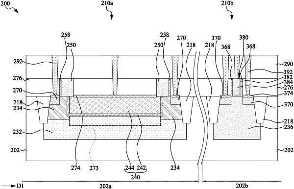
1. A semiconductor structure, comprising:
a substrate;
a doped region within the substrate;
a pair of source/drain regions extending along a first direction on opposite sides of the doped region;
a gate electrode disposed in the doped region, wherein the gate electrode has a plurality of first segments between the pair of source/drain regions and extending in parallel along the first direction; and
a protection structure over the substrate and at least partially overlapping the gate electrode.
|