| CPC H01L 29/7786 (2013.01) [H01L 23/481 (2013.01); H01L 29/2003 (2013.01)] | 13 Claims |
|
1. A semiconductor device, comprising:
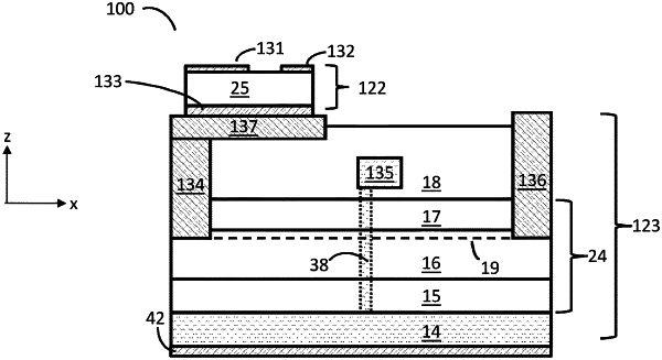
a III-N device comprising a conductive substrate on a first side of a III-N material structure that includes an electrically insulating buffer layer, and a first gate, a first source, and a first drain over a second side of the III-N material structure opposite the substrate, wherein the first source is electrically separated from the conductive substrate by the electrically insulating buffer layer;
a field effect transistor (FET) comprising a second semiconductor material structure, and second gate, a second source, and a second drain, the second source and the second gate being over an opposite side of the second semiconductor material structure from the second drain, wherein the second drain of the FET is physically mounted and electrically connected to a source pad of the first source of the III-N device; and
a via-hole extending through a portion of the III-N material structure and terminating at the conductive substrate, wherein the first gate is electrically connected to the conductive substrate by a metal layer formed in the via-hole.
|