| CPC H01L 29/66833 (2013.01) [H01L 21/31144 (2013.01); H01L 21/32137 (2013.01); H01L 29/0649 (2013.01); H01L 29/42344 (2013.01); H01L 29/792 (2013.01); H10B 43/35 (2023.02); H10B 43/40 (2023.02)] | 20 Claims |
|
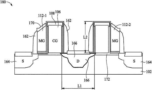
1. A method for making a semiconductor device, comprising:
patterning a first gate material layer and a gate insulating film over a substrate, the first gate material layer comprising a first gate material, the gate insulating film disposed on the first gate material layer;
forming a second gate material layer over the substrate, the gate insulating film, and side walls of the first gate material layer, the second gate material layer comprising a second gate material;
etching the second gate material layer to expose the substrate and the gate insulating film and provide a portion of the second gate material layer along each of the side walls of the first gate material layer;
etching the gate insulating film and the first gate material layer, after the second gate material layer is formed and etched, so as to form a plurality of gate structures; and
forming a protective layer over the substrate before etching the gate insulating film and the first gate material layer, the protective layer covering the first gate material layer, the gate insulating film, and the portion of the second gate material layer along each of the side walls of the first gate material layer.
|