| CPC H01L 29/6656 (2013.01) [H01L 29/1033 (2013.01); H01L 29/42376 (2013.01); H01L 29/66553 (2013.01); H01L 29/78696 (2013.01); H01L 21/28141 (2013.01); H01L 21/823468 (2013.01); H01L 29/1037 (2013.01); H01L 29/66719 (2013.01); H01L 29/7727 (2013.01)] | 17 Claims |
|
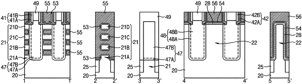
1. A semiconductor device, comprising:
a first active region defined on a substrate;
a first gate electrode across the first active region;
a first drain region in the first active region at a position adjacent to the first gate electrode;
an undercut region between the first active region and a metal portion of the first gate electrode;
a first gate spacer on a side surface of the first gate electrode and protruding into the undercut region, wherein the first gate spacer includes
an upper portion on the side surface of the first gate electrode, and
a lower portion extending from the upper portion into the undercut region,
wherein the first active region comprises a plurality of channel regions, each of the plurality of channel regions being in contact with the first drain region, and
wherein the first gate electrode surrounds a top surface, a side surface, and a bottom surface of at least one of the plurality of channel regions; and
a first gate dielectric layer between the first gate electrode and the plurality of channel regions and extending between the first gate electrode and the first gate spacer, the first gate dielectric layer being in contact with a side surface and a top surface of the lower portion,
wherein the undercut region is between the metal portion of the first gate electrode and an uppermost channel region of the plurality of channel regions.
|