| CPC H01L 29/66545 (2013.01) [H01L 21/2815 (2013.01); H01L 21/823418 (2013.01); H01L 21/823431 (2013.01); H01L 21/823437 (2013.01); H01L 21/823481 (2013.01); H01L 27/0886 (2013.01); H01L 29/0649 (2013.01); H01L 29/41791 (2013.01); H01L 29/6653 (2013.01); H01L 29/6656 (2013.01); H01L 29/6681 (2013.01); H01L 29/66795 (2013.01); H01L 29/785 (2013.01); H01L 21/823468 (2013.01)] | 20 Claims |
|
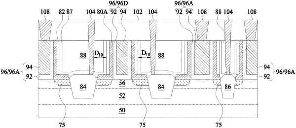
1. A device comprising:
a semiconductor fin over a substrate;
a first gate stack overlapping with the semiconductor fin in a plan view;
a first epitaxial source/drain region adjacent to the first gate stack and extending into the semiconductor fin;
a first spacer structure laterally interposed between a sidewall of the first gate stack and the first epitaxial source/drain region, the first spacer structure comprising:
a first L-shaped spacer along the sidewall of the first gate stack; and
a second spacer along an outer sidewall of a vertical portion of the first L-shaped spacer, a lateral portion of the first L-shaped spacer extending from an outer sidewall of the second spacer to the first epitaxial source/drain region; and
a conductive feature adjacent the first gate stack and in physical contact with a top surface of the first epitaxial source/drain region, a sidewall of the conductive feature being laterally spaced apart from the outer sidewall of the second spacer by a first distance of between about 10 nm and about 25 nm, the sidewall of the conductive feature facing the outer sidewall of the second spacer.
|