| CPC H01L 29/4908 (2013.01) [H01L 21/02603 (2013.01); H01L 21/28088 (2013.01); H01L 21/823807 (2013.01); H01L 21/823814 (2013.01); H01L 21/823842 (2013.01); H01L 21/823864 (2013.01); H01L 21/823871 (2013.01); H01L 27/092 (2013.01); H01L 29/0673 (2013.01); H01L 29/42392 (2013.01); H01L 29/66545 (2013.01); H01L 29/66553 (2013.01); H01L 29/66742 (2013.01); H01L 29/78696 (2013.01)] | 20 Claims |
|
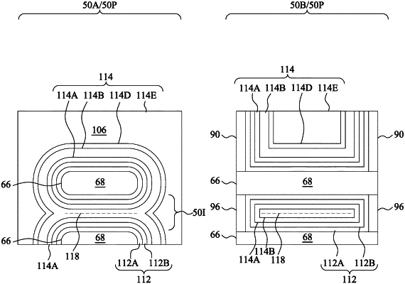
1. A device comprising:
a first nanostructure;
a second nanostructure;
a gate dielectric layer wrapped around the first nanostructure and the second nanostructure;
a tungsten-free work function tuning layer wrapped around the gate dielectric layer;
a tungsten-containing work function tuning layer wrapped around the tungsten-free work function tuning layer, an area between the first nanostructure and the second nanostructure being completely filled by respective portions of the tungsten-containing work function tuning layer, the tungsten-free work function tuning layer, and the gate dielectric layer, a first material of the tungsten-containing work function tuning layer having a lower resistivity than a second material of the tungsten-free work function tuning layer; and
a fill layer on the tungsten-containing work function tuning layer.
|