| CPC H01L 29/41775 (2013.01) [H01L 21/823814 (2013.01); H01L 21/823821 (2013.01); H01L 21/823878 (2013.01); H01L 27/0924 (2013.01)] | 20 Claims |
|
1. A semiconductor device, comprising:
a substrate including a first active region and a second active region that are spaced apart from each other in a first direction;
a device isolation layer on the substrate, the device isolation layer defining a first active pattern on the first active region and a second active pattern on the second active region;
a first gate electrode and a second gate electrode that run across the first active region and the second active region, the first gate electrode and the second gate electrode being aligned with each other in the first direction;
a first source/drain pattern and a second source/drain pattern on each of the first active pattern and the second active pattern;
a first active contact that extends in the first direction and connects the first source/drain pattern and the second source/drain pattern to each other; and
a gate cutting pattern between the first gate electrode and the second gate electrode,
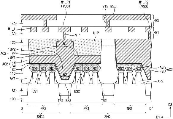
wherein an upper portion of the first active contact includes a first upper dielectric pattern on the first active region and a second upper dielectric pattern on the second active region,
wherein a minimum width at a portion of the first active contact is a first width, the portion of the first active contact being between the first upper dielectric pattern and the second upper dielectric pattern,
wherein a minimum width of the gate cutting pattern is a second width, and
wherein a ratio of the first width to the second width is in a range of about 0.8 to about 1.2.
|