| CPC H01L 29/40111 (2019.08) [H01L 29/6684 (2013.01); H01L 29/78391 (2014.09); H10B 51/00 (2023.02)] | 20 Claims |
|
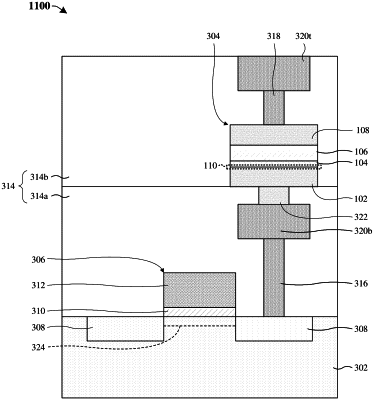
1. A method for forming an integrated circuit (IC), comprising:
forming a first electrode layer comprising a first metal over a substrate;
performing a first atomic layer deposition (ALD) pulse that exposes the first electrode layer to oxygen atoms;
exposing the first electrode layer to a first temperature, wherein the first temperature causes the first electrode layer to react with the oxygen atoms to form a seed structure over the first electrode layer; and
performing a series of ALD pulses at a second temperature to form a ferroelectric structure over the seed structure, wherein the second temperature is less than the first temperature and wherein the ferroelectric structure is configured to store a data state.
|