| CPC H01L 29/0847 (2013.01) [H01L 29/0653 (2013.01); H01L 29/66568 (2013.01); H01L 29/7848 (2013.01); H01L 29/78618 (2013.01)] | 18 Claims |
|
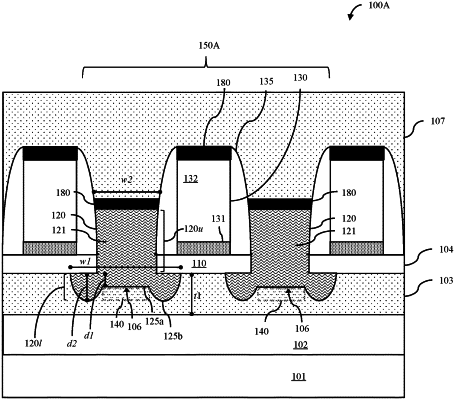
1. A structure comprising:
an insulator layer;
a semiconductor layer on the insulator layer; and
a transistor comprising:
source/drain regions extending through the semiconductor layer and into the insulator layer; and
a channel region in the semiconductor layer positioned laterally between the source/drain regions,
wherein each source/drain region has a first portion within the insulator layer and a second portion within the semiconductor layer,
wherein the first portion has an end section adjacent to the channel region, and an additional section positioned laterally adjacent to the end section and further aligned below the second portion,
wherein the additional section extends a first depth into the insulator layer and the end section extends a second depth into the insulator layer,
wherein the second depth is greater than the first depth, and
wherein the semiconductor layer extends laterally over the end section of the first portion to the second portion.
|