| CPC H01L 29/0673 (2013.01) [H01L 29/7827 (2013.01)] | 20 Claims |
|
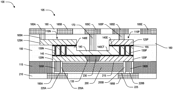
1. A semiconductor arrangement, comprising:
a first source pad formed over a semiconductor layer;
a first nanosheet contacting the first source pad;
a gate pad adjacent the first nanosheet;
a first drain pad over the gate pad and contacting the first nanosheet;
a backside interconnect line under the gate pad and the first source pad; and
a backside gate contact contacting the backside interconnect line and the gate pad.
|