| CPC H01L 29/0673 (2013.01) [H01L 27/0924 (2013.01)] | 20 Claims |
|
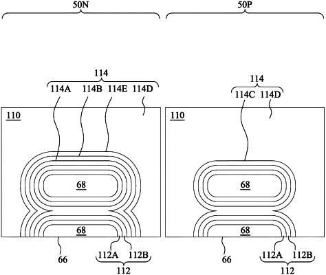
1. A device comprising:
nanostructures on a substrate, the nanostructures comprising a channel region;
a gate dielectric layer wrapping around each of the nanostructures;
a first work function tuning layer on the gate dielectric layer, the first work function tuning layer comprising a first n-type work function metal, aluminum, and carbon, the first n-type work function metal comprising zirconium, hafnium, or niobium;
a glue layer on the first work function tuning layer; and
a fill layer on the glue layer.
|