| CPC H01L 28/40 (2013.01) [H01L 21/76879 (2013.01); H01L 27/0805 (2013.01); H01L 28/90 (2013.01); H01L 29/945 (2013.01)] | 20 Claims |
|
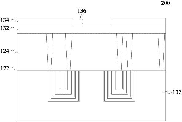
1. A method of making a semiconductor device, the method comprising:
etching a substrate to define a first trench and a second trench;
depositing a first number M of capacitor layer pairs in the first trench, wherein each of the first number M of capacitor layer pairs comprises:
a first dielectric layer, and
a first conductive layer;
depositing a second number N of capacitor layer pairs in the second trench, wherein the second number N is different from the first number M, and each of the second number N of capacitor layer pairs comprises:
a second dielectric layer, and
a second conductive layer; and
planarizing the first number M of capacitor layer pairs and the second number N of capacitor layer pairs to expose the substrate.
|