| CPC H01L 27/1464 (2013.01) [H01L 27/14623 (2013.01); H01L 27/14627 (2013.01); H01L 27/14632 (2013.01); H01L 27/14687 (2013.01); H01L 31/02164 (2013.01)] | 20 Claims |
|
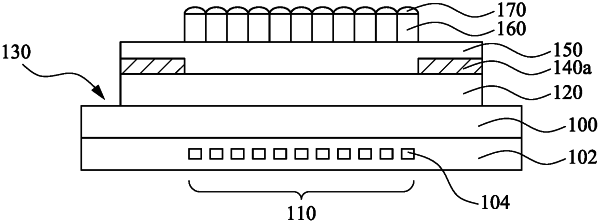
1. A method of manufacturing a backside illuminated image sensor device, the method comprising:
forming a dielectric layer on a back surface of a semiconductor substrate, wherein the semiconductor substrate has an pixel array formed on a front surface of the semiconductor substrate;
patterning the dielectric layer to form a plurality of scribe lines surrounding the pixel array;
forming a conductive shielding layer on the dielectric layer;
patterning the conductive shielding layer to expose the scribe lines;
forming a dielectric buffer layer on the patterned conductive shielding layer and the dielectric layer;
forming a color filter layer on the dielectric buffer layer; and
forming a microlens layer on the color filter layer.
|