| CPC H01L 27/14629 (2013.01) [H01L 27/14685 (2013.01); H01L 27/1463 (2013.01); H01L 27/1464 (2013.01); H01L 27/14623 (2013.01)] | 20 Claims |
|
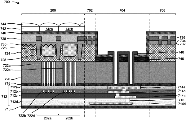
15. A method, comprising:
forming, for a pixel sensor of a pixel array included in an image sensor, a plurality of openings through an un-doped silicate glass (USG) layer of the image sensor and in an interlayer dielectric (ILD) layer of the image sensor;
forming an inter-metal dielectric (IMD) layer on the USG layer,
wherein the IMD layer closes the plurality of openings to form a plurality of air gap reflection structures of the pixel sensor, and
wherein the plurality of air gap reflection structures are formed to have an aspect ratio, between a depth of an air gap reflection structure of the plurality of air gap reflection structures and a width of the air gap reflection structure, greater than approximately 2; and
forming a photodiode in a silicon layer above the ILD layer,
wherein the photodiode is formed over the plurality of air gap reflection structures.
|