| CPC H01L 27/14623 (2013.01) [H01L 27/14683 (2013.01)] | 20 Claims |
|
1. A method for fabricating an image sensor device, comprising:
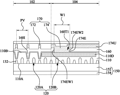
forming a plurality of photosensitive pixels in a substrate and a plurality of reference photosensitive pixels around the photosensitive pixels;
depositing a dielectric layer over the substrate;
etching the dielectric layer, resulting in a first trench in the dielectric layer and laterally surrounding the photosensitive pixels; and
forming a light blocking structure in the first trench, such that the light blocking structure laterally surrounds the photosensitive pixels, and such that a bottommost surface of the light blocking structure is in contact with the substrate and overlaps the reference photosensitive pixels from a top view.
|