| CPC H01L 27/14603 (2013.01) [G01L 1/18 (2013.01); H01L 27/14618 (2013.01); H01L 27/14621 (2013.01); H01L 27/14627 (2013.01); H01L 27/14636 (2013.01); H01L 27/14645 (2013.01)] | 7 Claims |
|
1. A semiconductor element comprising:
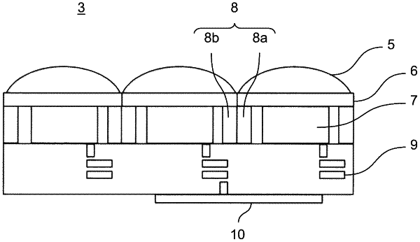
a plurality of microlenses provided on an upper surface of a main layer to collect light;
a plurality of conductive electrodes provided on a lower surface of the main layer;
at least one photoelectric converter to which the light collected by the plurality of microlenses is guided provided in the main layer;
a strain sensor electrically connected to the plurality of conductive electrodes via internal wiring and provided in the main layer with the photoelectric converter, the strain sensor being configured to detect a strain using a piezoresistive effect in which electrical resistance changes when a mechanical stress is applied; and
a color filter provided in the main layer and between the plurality of microlenses and the photoelectric converter to filter the light collected by the plurality of microlenses.
|