| CPC H01L 27/1255 (2013.01) [H10K 59/122 (2023.02); H10K 59/124 (2023.02); H10K 59/1213 (2023.02); H10K 59/131 (2023.02); G09G 3/3266 (2013.01); G09G 2310/0202 (2013.01); G09G 2320/0233 (2013.01); G09G 2380/02 (2013.01); H01L 27/124 (2013.01); H01L 27/1248 (2013.01); H10K 59/1201 (2023.02)] | 7 Claims |
|
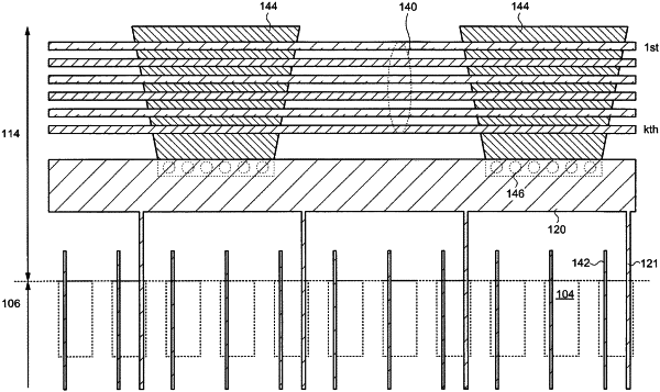
1. A TFT array substrate comprising:
a plurality of electrodes arranged in first to nth rows and first to mth columns;
first to nth scanning lines arranged in the respective first to nth rows; and
at least one first semiconductor film overlapping with at least one of the first to kth scanning lines selected from the first to nth scanning lines,
wherein an active region defined by the plurality of electrodes has a cutoff intersecting the first to kth rows,
the at least one first semiconductor film is located in the cutoff,
each of the plurality of electrodes is electrically connected to a transistor having a second semiconductor film,
the at least one first semiconductor film and the second semiconductor films exist in the same layer,
the at least one first semiconductor film includes a first impurity,
the second semiconductor film includes a second impurity different from the first impurity, and
n and m are each a natural number larger than 1, and k is a natural number smaller than n.
|