| CPC H01L 27/11807 (2013.01) [H01L 27/0207 (2013.01); H01L 2027/11861 (2013.01); H01L 2027/11866 (2013.01); H01L 2027/11885 (2013.01)] | 20 Claims |
|
1. An integrated circuit comprising:
a first standard cell comprising:
a first p-type transistor;
a first n-type transistor;
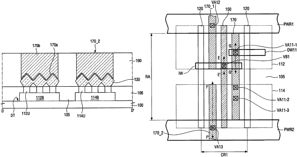
a first gate stack that extends in a second direction to intersect a first active region and a second active region that extends in a first direction;
at least two first extended source/drain contacts that extend in the second direction on a first side of the first gate stack;
a first normal source/drain contact that extends in the second direction on a second side of the first gate stack that is opposite the first side;
a first gate via that is connected to the first gate stack; and
a first source/drain via that is connected to the first normal source/drain contact;
a second standard cell that is adjacent the first standard cell in the first direction and comprises:
a second p-type transistor;
a second n-type transistor;
a second gate stack that extends in the second direction to intersect the first active region and the second active region; and
a second gate via that is connected to the second gate stack;
an input wiring of the first standard cell that extends in the first direction and is connected to the first gate via; and
an output wiring of the first standard cell that extends in the first direction and is at a same level as the input wiring to have a direct electrical connection between the first source/drain via and the second gate via,
wherein the first p-type transistor and the second p-type transistor are on the first active region,
wherein the first n-type transistor and the second n-type transistor are on the second active region.
|