| CPC H01L 27/0924 (2013.01) [H01L 21/823418 (2013.01); H01L 21/823431 (2013.01); H01L 29/66795 (2013.01); H01L 29/7851 (2013.01)] | 20 Claims |
|
1. A semiconductor device structure, comprising:
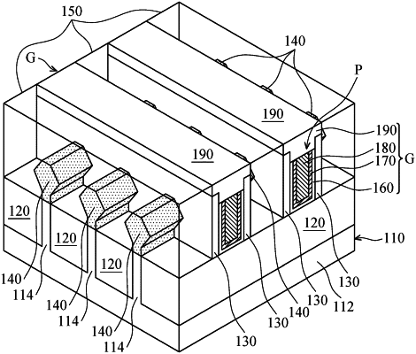
a substrate having a first fin structure;
a first source/drain structure over the first fin structure;
a first dielectric layer over the first source/drain structure and the substrate;
a first conductive contact structure in the first dielectric layer and over the first source/drain structure, and the first conductive contact structure has a substantially strip shape in a top view of the first conductive contact structure;
a second dielectric layer over the first dielectric layer and the first conductive contact structure;
a first conductive via structure passing through the second dielectric layer and connected to the first conductive contact structure, wherein the first conductive via structure has a first substantially strip shape in a top view of the first conductive via structure; and
a first conductive line over the first conductive via structure and the second dielectric layer, wherein the first conductive line is electrically connected to the first source/drain structure through the first conductive contact structure and the first conductive via structure.
|