| CPC H01L 27/0886 (2013.01) [H01L 21/7682 (2013.01); H01L 23/535 (2013.01); H01L 29/41791 (2013.01); H01L 29/42392 (2013.01); H01L 29/66795 (2013.01); H01L 29/7851 (2013.01)] | 20 Claims |
|
1. A method comprising:
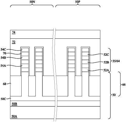
providing a first transistor structure, the first transistor structure comprising a semiconductor fin, a gate structure on the semiconductor fin, and a source/drain region in the semiconductor fin adjacent the gate structure;
forming a backside interconnect structure on a backside of the first transistor structure, wherein forming the backside interconnect structure comprises:
removing an isolation structure surrounding the semiconductor fin and the source/drain region;
forming first spacers along sidewalls of the semiconductor fin and the source/drain region;
etching the source/drain region using the first spacers as a mask; and
forming a dielectric layer surrounding the semiconductor fin, the source/drain region, and the first spacers.
|