| CPC H01L 27/0207 (2013.01) [H01L 21/31053 (2013.01); H01L 21/31111 (2013.01); H01L 21/32139 (2013.01); H01L 21/76224 (2013.01); H01L 21/823431 (2013.01); H01L 21/823437 (2013.01); H01L 21/823481 (2013.01); H01L 27/0886 (2013.01); H01L 29/0649 (2013.01); H01L 29/42372 (2013.01); H01L 29/4958 (2013.01); H01L 29/4966 (2013.01); H01L 21/0276 (2013.01); H01L 21/28556 (2013.01); H01L 21/823418 (2013.01); H01L 27/088 (2013.01); H01L 29/6656 (2013.01); H01L 29/66545 (2013.01); H01L 29/66636 (2013.01)] | 19 Claims |
|
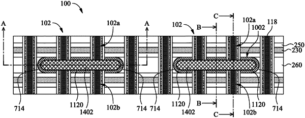
1. A semiconductor device, comprising:
a semiconductor substrate;
an isolation layer disposed on the semiconductor substrate;
a first active region and a second active region disposed at least partially above the isolation layer, wherein the first active region and the second active region each comprise a long axis and a short axis, wherein the long axes of the first and second active regions are substantially parallel and extend in a first direction;
a first gate structure and a second gate structure disposed on the isolation layer, the first active region, and the second active region, wherein the first gate structure and the second gate structure each comprise a long axis and a short axis, wherein the long axes of the first and second gate structures are substantially parallel and extend in a second direction, wherein the second direction is substantially perpendicular to the first direction; and
an isolation structure disposed on the isolation layer between the first and second active regions, the isolation structure being between and in contact with the first and second gate structures, wherein a thickness of the isolation structure varies.
|