| CPC H01L 25/0657 (2013.01) [H01L 21/0214 (2013.01); H01L 21/0217 (2013.01); H01L 21/02164 (2013.01); H01L 21/288 (2013.01); H01L 21/31051 (2013.01); H01L 21/3212 (2013.01); H01L 21/568 (2013.01); H01L 21/7684 (2013.01); H01L 21/76885 (2013.01); H01L 23/295 (2013.01); H01L 23/3107 (2013.01); H01L 23/3128 (2013.01); H01L 23/481 (2013.01); H01L 24/03 (2013.01); H01L 24/09 (2013.01); H01L 24/89 (2013.01); H01L 25/0652 (2013.01); H01L 25/50 (2013.01); H01L 21/561 (2013.01); H01L 23/49816 (2013.01); H01L 23/49822 (2013.01); H01L 23/49827 (2013.01); H01L 23/5389 (2013.01); H01L 2224/0231 (2013.01); H01L 2224/0239 (2013.01); H01L 2224/02373 (2013.01); H01L 2224/03002 (2013.01); H01L 2224/04105 (2013.01); H01L 2224/05025 (2013.01); H01L 2224/05124 (2013.01); H01L 2224/05147 (2013.01); H01L 2224/08145 (2013.01); H01L 2224/18 (2013.01); H01L 2224/80895 (2013.01); H01L 2224/80896 (2013.01); H01L 2224/81005 (2013.01); H01L 2224/82 (2013.01); H01L 2225/06524 (2013.01); H01L 2225/06527 (2013.01); H01L 2225/06541 (2013.01); H01L 2225/06548 (2013.01); H01L 2924/01022 (2013.01); H01L 2924/01029 (2013.01); H01L 2924/1431 (2013.01); H01L 2924/1432 (2013.01); H01L 2924/1433 (2013.01); H01L 2924/1434 (2013.01); H01L 2924/1436 (2013.01); H01L 2924/1437 (2013.01); H01L 2924/1461 (2013.01); H01L 2924/15311 (2013.01); H01L 2924/15331 (2013.01); H01L 2924/2011 (2013.01); H01L 2924/20106 (2013.01); H01L 2924/20107 (2013.01); H01L 2924/20108 (2013.01); H01L 2924/20109 (2013.01)] | 20 Claims |
|
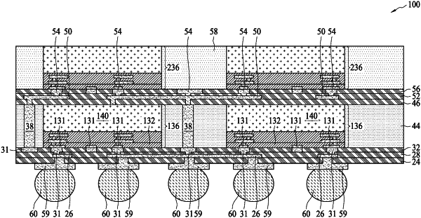
1. A method comprising:
providing a first carrier;
forming a conductive layer over the first carrier;
forming a plurality of metal bond pads over the conductive layer;
after forming the plurality of metal bond pads, forming a passivation layer over the conductive layer, the passivation layer surrounding the plurality of metal bond pads, wherein a first surface of the passivation layer is level with surfaces of the plurality of metal bond pads;
electrically coupling a plurality of electrode pads formed on an active surface of a semiconductor chip with the plurality of metal bond pads;
forming a molding compound over the first carrier and the plurality of metal bond pads;
removing the first carrier; and
forming a redistribution layer over the plurality of metal bond pads and a surface of the semiconductor chip opposite the active surface, the redistribution layer being electrically coupled to the plurality of metal bond pads.
|