| CPC H01L 24/81 (2013.01) [H01L 23/367 (2013.01); H01L 23/49816 (2013.01); H01L 23/49827 (2013.01); H01L 23/49833 (2013.01); H01L 23/552 (2013.01); H01L 23/60 (2013.01); H01L 24/09 (2013.01); H01L 25/0655 (2013.01); H01L 2224/08238 (2013.01); H01L 2224/16225 (2013.01); H01L 2224/81192 (2013.01); H01L 2924/014 (2013.01); H01L 2924/0105 (2013.01); H01L 2924/01014 (2013.01); H01L 2924/01028 (2013.01); H01L 2924/01029 (2013.01); H01L 2924/01047 (2013.01); H01L 2924/01082 (2013.01); H01L 2924/14 (2013.01); H01L 2924/1433 (2013.01); H01L 2924/1461 (2013.01); H01L 2924/1579 (2013.01); H01L 2924/15192 (2013.01); H01L 2924/15311 (2013.01); H01L 2924/15331 (2013.01); H01L 2924/15738 (2013.01); H01L 2924/15787 (2013.01); H01L 2924/19105 (2013.01)] | 1 Claim |
|
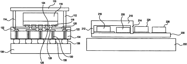
1. A method for mutually electromagnetically isolating first and second adjacent integrated circuit (IC) devices that are attached to a first side of a common bottom interposer by respective attaching structures that comprise small bumps, the method comprising:
attaching the common bottom interposer to a chip carrier with the first and second adjacent IC devices facing away from the chip carrier;
attaching a first top interposer to the common bottom interposer with the first top interposer covering the first IC device and with large bumps of the first top interposer contacting through-silicon vias (TSVs) of the common bottom interposer around all edges of the first IC device, wherein the TSVs of the common bottom interposer electrically connect a blanket metal shield of the first top interposer to a ground of the chip carrier; and
attaching a second top interposer to the common bottom interposer with the second top interposer covering the second IC device and with large bumps of the second top interposer contacting through-silicon vias (TSVs) of the common bottom interposer around all edges of the second IC device, wherein the TSVs of the common bottom interposer electrically connect a blanket metal shield of the second top interposer to a ground of the chip carrier.
|